Chinese electronics giant Huawei today unveiled a new chip design framework it says will help close the gap with global leaders like TSMC and Nvidia, despite ongoing U.S. sanctions.
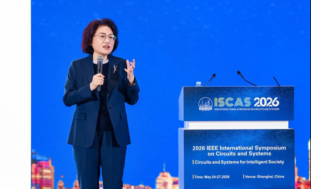
At the IEEE International Symposium on Circuits and Systems in Shanghai, Huawei board member He Tingbo introduced a proprietary “LogicFolding” architecture and a new “Tau Scaling Law” to replace Moore’s Law. The approach prioritizes signal speed over transistor size, allowing advanced chip performance without the need for banned EUV lithography machines.
Huawei has quietly refined the architecture for over six years, producing 381 test chips. The first commercial product will be a Kirin smartphone processor, debuting this fall in the Mate 90 handset. The company targets 1.4nm-class chips with a 55% increase in transistor density by 2031.
Analysts call it an alternative path forward amid supply chain challenges. Shares of China’s Semiconductor Manufacturing International Co. surged over 19% on the news.